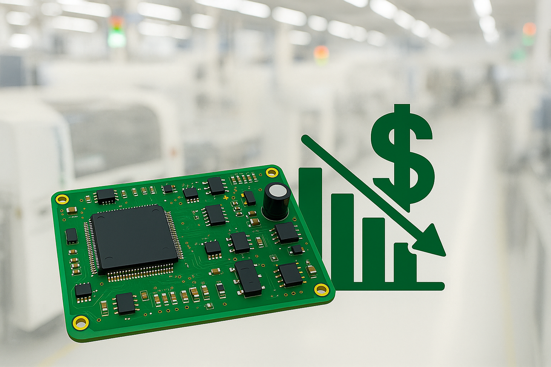
Cost Reduction in Hardware Projects
- Milton M Xavier
- Hardware
- August 31, 2025
Table of Contents
Concept
In this post, we will discuss actions you can take in your project to reduce the cost of manufacturing printed circuit boards (PCBs) and the cost of assembly, i.e., mounting components on the board.
For those already working in the field developing embedded systems, these concepts are straightforward. However, if you don’t directly work in development but are in a position to decide on redesigning a project or at least provide input, pay attention to these four points I’ll mention regarding your company’s projects or the company you work for. Depending on the annual production volume, the savings can be significant.
Let’s dive in!
Printed Circuit Board Size
We define the size of the PCB based on two main criteria:
- The number and size of components: This means that PCBs designed for power processing, which use electrolytic capacitors and switches like MOSFETs or IGBTs, tend to require a larger size than general-purpose boards or IoT devices.
- The mechanics where the PCB will be mounted: If you use an enclosure with standard mounting holes, it may be necessary to extend the PCB area to utilize the pre-existing holes in the enclosure.
- At the moment, no other criteria for defining PCB size come to mind. If you have any additional ones, please comment at the end of this content.
Now, if you sell 5 units of this product per month, the cost difference won’t significantly impact your operation. But what if you sell 10,000 units per month? A 30% reduction in PCB area basically means a 30% reduction in its cost. Let me explain further. These are the factors that determine the manufacturing cost of a PCB:
- Material used: Phenolic, composite, fiberglass, etc.
- Number of layers: Single-sided, double-sided, or multilayer (4 or more layers).
- Smallest drill hole diameter: Manufacturers generally work well with a minimum drill hole diameter of 0.3 mm. Anything smaller increases the PCB manufacturing cost. (If I recall correctly, someone from a PCB manufacturing company in Brazil explained that when the drill hole diameter is very small, instead of drilling 10 boards at once in the drilling machine, they need to drill fewer at a time, increasing the number of hours required for production. Additionally, very thin drills break easily).
- Smallest track width and spacing between tracks: Manufacturers work well with values greater than 6 mils for track width and spacing. Smaller values make the process more difficult, as tracks can break easily during the etching process, and shorts between tracks are more likely to occur.
- Copper thickness: The thicker the copper (1 oz, 2 oz, etc.), the higher the PCB cost. (Curiously, copper thickness is not expressed directly in micrometers but in ounces per square foot (oz/ft²). So, the market decided to mix weight with area to describe thickness. In the end, 1 oz/ft² is equivalent to about 35 µm of copper. Market quirks…).
Now let’s imagine the following characteristics for your project: a fiberglass (FR4) PCB, double-sided, 1 oz, smallest drill hole diameter of 0.5 mm, and smallest track width and spacing of 8 mils. The cost per square meter is x. The more boards that fit per square meter, the lower the individual cost per unit.
If 1 board fits per m², the cost per board is x. If 2 boards fit per m², the cost is \(\dfrac{x}{2}\). If 1,000 boards fit per m², the cost is \(\dfrac{x}{1000}\).
That’s basically it. You need to consider false edges for panelization, the spacing between boards within the panel to facilitate production, etc. But, in general, that’s how it works.
Therefore, if there’s a possibility to reduce the PCB size, do it.
Avoid PTH Components
If the application the PCB is intended for involves communication, signal processing, or digital electronics, there’s no reason to use PTH components. It’s that simple. The scenario is different for power processing boards.
Using PTH components requires an additional step in the production process: PTH assembly, which, in most manufacturing companies, is done manually.
While SMD assembly requires only one operator to manage the entire line (loading blank boards at the start, handling the solder paste printer, managing pick-and-place machines for SMD component placement, overseeing the reflow oven, and finally waiting for the board to cool at the end of the line before sending it to testing or storage), PTH assembly requires more people to manually insert components through the board’s holes and then pass it through the wave solder, a solder bath with a conveyor that solders the component pins to the board. This manual process requires more people, is time-consuming, and more prone to errors, which may require rework. That’s why it’s more expensive.
So, if your application allows, switch everything to SMD components. Assembly will be done on a 100% automated line, which is much faster, cheaper, and more efficient.
Warning
Another important point: SMD components tend to be cheaper compared to their PTH equivalents. If you use a 10 kΩ PTH resistor, its SMD equivalent is cheaper.
Avoid Components on the Bottom Side
I know. High-frequency applications with processors and memories in BGA packages require capacitors on the bottom side under these components.
Is your application high-frequency, and do you use processors or memories? No? Then remove all components from the bottom side.
Unless you have space constraints: your enclosure is too small.
Otherwise, it’s a waste of money, as the board needs to go through the SMT line twice—once to assemble components on the TOP side and again for the BOTTOM side. Additionally, bottom-side components require them to be glued to the board before wave soldering. This process is not only expensive but also labor-intensive, as some components may be “torn off” during wave soldering.
In short: it’s an extra process, additional materials like glue, and it increases the risk of issues. If it’s not necessary, avoid it.
Avoid Obsolete Components
I won’t explain this point in detail. I’ll just give an example:
ATMEGA8A-AU microcontroller, an obsolete 32-pin, 8-bit microcontroller running at 16 MHz, with 8 kB of flash memory, 1 kB of RAM, and 512 B of EEPROM for permanent data storage. It costs, at Mouser, for 100 units as of this post’s date, a whopping US$2.11 per unit.

STM32C031K4T6 microcontroller - a modern 32-pin, 32-bit microcontroller running at 48 MHz, with 16 kB of flash memory and 12 kB of RAM. It doesn’t have EEPROM, but you can write permanent data to the flash memory. It costs, at Mouser, for 100 units as of this post’s date, US$0.722 per unit.

I don’t think I need to say anything more (“write” would be the more accurate term, but “say” sounds cooler).
Summary and Conclusion
Quick guide to reducing PCB and assembly costs:
Carefully plan the PCB:
- More boards per panel = lower cost per unit.
- Tracks ≥ 6 mils and holes ≥ 0.3 mm help keep costs low.
- 1 oz/ft² (≈ 35 µm) is sufficient for most projects. Avoid overdoing it without necessity.
Prefer SMD over PTH:
- Faster, cheaper assembly with less rework.
- Use PTH only where strictly necessary (connectors, high power, etc.).
Avoid components on the bottom side:
- Each extra side assembled increases SMT line costs.
- Use only if there’s no space on the top or in special cases (high frequency, BGA).
Avoid obsolete components:
- Old components are often expensive and hard to find.
- Replace them with modern, available equivalents.
Done! With the money saved by the end of the year, invest in new projects or equipment. Help your company grow and count on Greenboard as your engineering partner.